- 您现在的位置:买卖IC网 > Sheet目录2003 > LTC1420IGN#TRPBF (Linear Technology)IC ADC 12BIT 10MSPS SAMPL 28SSOP
6
LTC1420
1420fa
TYPICAL PERFOR A CE CHARACTERISTICS
UW
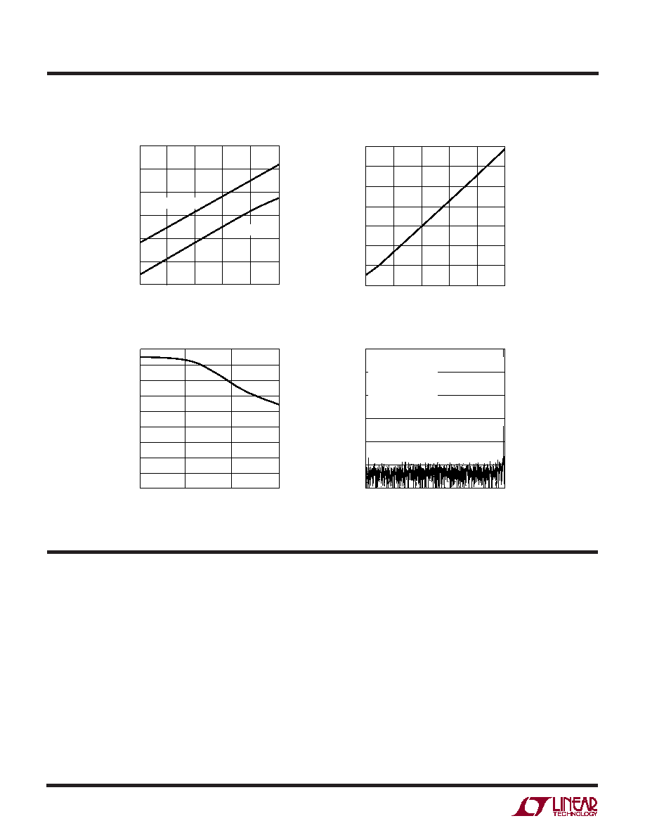
IDD vs Clock Frequency
CLOCK FREQUENCY (MHz)
0
40
I DD
(mA)
42
44
46
48
50
52
246
8
1420 G10
10
VREF = 4.096V
VREF = 2.048V
CLOCK FREQUENCY (MHz)
0
1.0
1.2
1.4
8
6
1420 G11
0.8
0.6
24
10
0.4
0.2
0
I SS
(mA)
ISS vs Clock Frequency
CMRR vs Input Frequency
INPUT FREQUENCY (MHz)
0.01
0
CMRR
(dB)
10
30
40
50
1
90
1420 G12
20
0.1
10
60
70
80
+AIN (Pin 1): Positive Analog Input.
–AIN (Pin 2): Negative Analog Input.
VCM (Pin 3): 2.5V Reference Output.Optional input com-
mon mode for single supply operation. Bypass to GND
with a 1F to 10F ceramic.
SENSE (Pin 4): Reference Programming Pin. Ground
selects VREF = 4.096V. Short to VREF for 2.048V. Connect
SENSE to VDD to drive VREF with an external reference.
VREF (Pin 5): DAC Reference. Bypass to GND with a 1F to
10F ceramic.
GND (Pin 6): DAC Reference Ground.
VDD (Pin 7): Analog 5V Supply. Bypass to GND with a 1F
to 10F ceramic.
GND (Pin 8): Analog Power Ground.
D11 to D0 (Pins 9 to 20): Data Outputs. The output format
is two’s complement.
OGND (Pin 21): Output Logic Ground. Tie to GND.
OVDD (Pin 22): Positive Supply for the Output Logic.
Connect to Pin 23 for 5V logic. If not shorted to Pin 23,
bypass to GND with a 1F ceramic.
PIN FUNCTIONS
UU
U
LTC1420 Nonaveraged 4096 Point FFT
FREQUENCY (MHz)
0
–120
AMPLITUDE
(dB)
–100
–80
–60
–40
–20
0
123
4
1420 G13
5
fSAMPLE = 10Msps
fIN = 5.048828125MHz
SFDR = 83.2dB
SINAD = 71dB
VIN = 4VP-P
±5V SUPPLIES
发布紧急采购,3分钟左右您将得到回复。
相关PDF资料
LTC1426IS8#TR
IC DAC PWM 6BIT DUAL MCPWR 8SOIC
LTC1427CS8-50#TRPBF
IC D/A CONV 10BIT W/SMBUS 8-SOIC
LTC1428CS8-50#TRPBF
IC D/A CONV 8BIT SINK OUT 8-SOIC
LTC1446LIS8#TRPBF
IC D/A CONV 12BIT R-R DUAL 8SOIC
LTC1448IS8#TRPBF
IC D/A CONV 12BIT R-R DUAL 8SOIC
LTC1450LIG#TR
IC DAC 12BIT R-R PAR MPWR 24SSOP
LTC1451IS8#TRPBF
IC D/A CONV 12BIT R-R 8-SOIC
LTC1454LCN
IC D/A CONV 12BIT R-R DUAL 16DIP
相关代理商/技术参数
LTC1421CG
功能描述:IC CONTROLLER HOT SWAP 24-SSOP RoHS:否 类别:集成电路 (IC) >> PMIC - 热交换 系列:- 产品培训模块:Lead (SnPb) Finish for COTS
Obsolescence Mitigation Program 标准包装:119 系列:- 类型:热交换控制器 应用:通用型,PCI Express? 内部开关:无 电流限制:- 电源电压:3.3V,12V 工作温度:-40°C ~ 85°C 安装类型:表面贴装 封装/外壳:80-TQFP 供应商设备封装:80-TQFP(12x12) 包装:托盘 产品目录页面:1423 (CN2011-ZH PDF)
LTC1421CG#PBF
功能描述:IC CONTROLLER HOT SWAP 24-SSOP RoHS:是 类别:集成电路 (IC) >> PMIC - 热交换 系列:- 产品培训模块:Lead (SnPb) Finish for COTS
Obsolescence Mitigation Program 标准包装:119 系列:- 类型:热交换控制器 应用:通用型,PCI Express? 内部开关:无 电流限制:- 电源电压:3.3V,12V 工作温度:-40°C ~ 85°C 安装类型:表面贴装 封装/外壳:80-TQFP 供应商设备封装:80-TQFP(12x12) 包装:托盘 产品目录页面:1423 (CN2011-ZH PDF)
LTC1421CG#TR
功能描述:IC CONTROLLER HOTSWAP ADJ 24SSOP RoHS:否 类别:集成电路 (IC) >> PMIC - 热交换 系列:- 产品培训模块:Lead (SnPb) Finish for COTS
Obsolescence Mitigation Program 标准包装:119 系列:- 类型:热交换控制器 应用:通用型,PCI Express? 内部开关:无 电流限制:- 电源电压:3.3V,12V 工作温度:-40°C ~ 85°C 安装类型:表面贴装 封装/外壳:80-TQFP 供应商设备封装:80-TQFP(12x12) 包装:托盘 产品目录页面:1423 (CN2011-ZH PDF)
LTC1421CG#TRPBF
功能描述:IC CONTROLLER HOT SWAP 24-SSOP RoHS:是 类别:集成电路 (IC) >> PMIC - 热交换 系列:- 产品培训模块:Lead (SnPb) Finish for COTS
Obsolescence Mitigation Program 标准包装:119 系列:- 类型:热交换控制器 应用:通用型,PCI Express? 内部开关:无 电流限制:- 电源电压:3.3V,12V 工作温度:-40°C ~ 85°C 安装类型:表面贴装 封装/外壳:80-TQFP 供应商设备封装:80-TQFP(12x12) 包装:托盘 产品目录页面:1423 (CN2011-ZH PDF)
LTC1421CG1
制造商:Linear Technology 功能描述:
LTC1421CG-2.5
功能描述:IC CONTROLLER HOT SWAP 24-SSOP RoHS:否 类别:集成电路 (IC) >> PMIC - 热交换 系列:- 产品培训模块:Lead (SnPb) Finish for COTS
Obsolescence Mitigation Program 标准包装:119 系列:- 类型:热交换控制器 应用:通用型,PCI Express? 内部开关:无 电流限制:- 电源电压:3.3V,12V 工作温度:-40°C ~ 85°C 安装类型:表面贴装 封装/外壳:80-TQFP 供应商设备封装:80-TQFP(12x12) 包装:托盘 产品目录页面:1423 (CN2011-ZH PDF)
LTC1421CG-2.5#PBF
功能描述:IC CONTROLLER HOT SWAP 24-SSOP RoHS:是 类别:集成电路 (IC) >> PMIC - 热交换 系列:- 标准包装:50 系列:- 类型:热交换控制器 应用:-48V 远程电力系统,AdvancedTCA ? 系统,高可用性 内部开关:无 电流限制:可调 电源电压:11.5 V ~ 14.5 V 工作温度:-40°C ~ 85°C 安装类型:表面贴装 封装/外壳:10-TFSOP,10-MSOP(0.118",3.00mm 宽) 供应商设备封装:10-MSOP 包装:管件
LTC1421CG-2.5#TR
功能描述:IC CONTROLLER HOTSWP 2.5V 24SSOP RoHS:否 类别:集成电路 (IC) >> PMIC - 热交换 系列:- 产品培训模块:Lead (SnPb) Finish for COTS
Obsolescence Mitigation Program 标准包装:119 系列:- 类型:热交换控制器 应用:通用型,PCI Express? 内部开关:无 电流限制:- 电源电压:3.3V,12V 工作温度:-40°C ~ 85°C 安装类型:表面贴装 封装/外壳:80-TQFP 供应商设备封装:80-TQFP(12x12) 包装:托盘 产品目录页面:1423 (CN2011-ZH PDF)